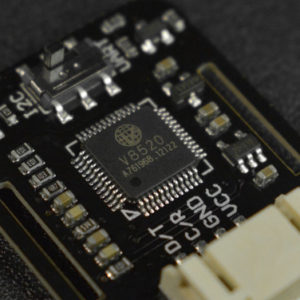
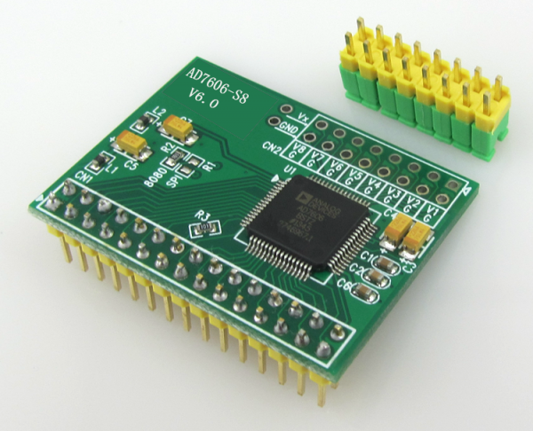
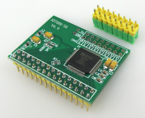
AD7606 高精度 16位ADC / 200Ksps 8Ch / 平行 SPI通訊
NT$840 未稅
AD7606 高精度 16位ADC / 200Ksps 8Ch / 平行 SPI通訊
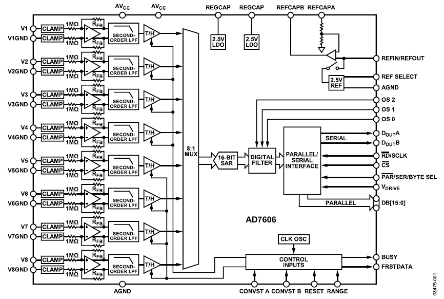
AD7606的配置很簡單,它沒有內部寄存器。量程範圍和過採樣參數是通過外部IO控制的。 採樣速率由MCU或DSP提供的脈衝頻率控制。 AD7606必須使用單5V供電。 AD7606和MCU之間的通信接口電平由VIO引腳控制。也就是說VIO必須接單片機的電源,可以是3.3V也可以是5V。
尚有庫存
- 商品說明
商品說明
AD7606 高精度 16位ADC / 200Ksps 8Ch / 平行 SPI通訊
- 使用AD7606 高精度16位ADC芯片
- 8路模擬輸入。阻抗1M歐姆。【無需負電源,無需前端模擬運放電路,可直接接傳感器輸出】
- 輸入範圍正負5V,正負10V。可通過IO控制量程。
- 分辨率16位。
- 最大採樣頻率200Ksps。支持8檔過採樣設置(可以有效降低抖動)
- 內置基準
- 單5V供電
- SPI接口或16位總線接口。接口IO電平可以是5V或3.3V
原廠技術文件
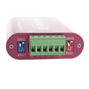
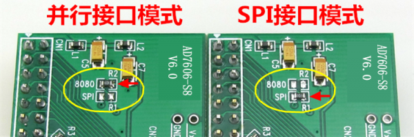
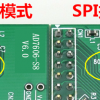
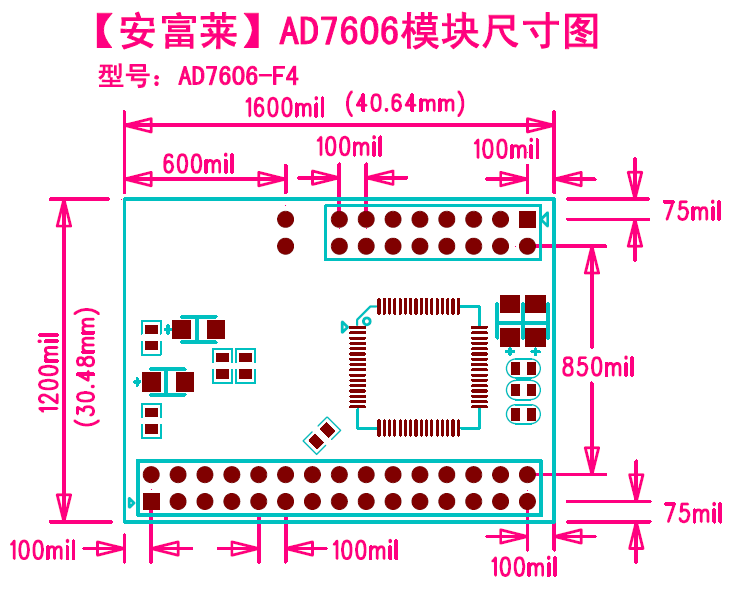
如果用SPI介面模式,需要修改 R1 R2電阻配置。
並口模式跳線: R1 懸空(不貼),R2貼10K電阻
SPI介面模式跳線:R1 貼10K電阻, R2 懸空(不貼)
AD7606 的配置很簡單,它沒有內部寄存器。量程範圍和過採樣參數是通過外部IO控制的。
採樣速率由MCU或DSP提供的脈衝頻率控制。
AD7606 必須使用單5V供電。
AD7606 和MCU之間的通信介面電平由VIO引腳控制。也就是說 VIO必須接單片機的電源,可以是3.3V也可以是5V。
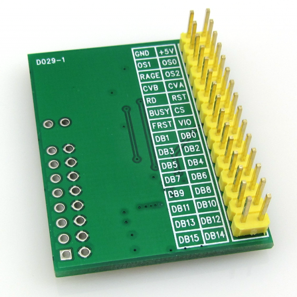
【模組引腳說明】
OS2 OS1 OS2 : 的組合狀態選擇過採樣模式。
000表示無過採樣,最大200Ksps採樣速率。
001表示2倍過採樣, 也就是硬體內部採集2個樣本求平均
010表示4倍過採樣, 也就是硬體內部採集4個樣本求平均
011表示8倍過採樣, 也就是硬體內部採集8個樣本求平均
100表示16倍過採樣, 也就是硬體內部採集16個樣本求平均
101表示32倍過採樣, 也就是硬體內部採集32個樣本求平均
110表示64倍過採樣, 也就是硬體內部採集64個樣本求平均
過採樣倍率越高,ADC轉換時間越長,可得到的最大採樣頻率就越低。
CVA,CVB : 啟動AD轉換的控制信號。CVA決定1-4通道,CVB決定5-8通道。
2個信號可以錯開短暫的時間。一般情況可以將CVA,CVB並聯在一起。
RAGE : 量程範圍選擇。0表示正負5V, 1表示正負10V.
RD : 讀信號
RST : 複位信號
BUSY : 忙信號
CS : 片選信號
FRST : 第1個通道樣本的指示信號
VIO : 通信介面電平
DB0-DB15 : 數據匯流排
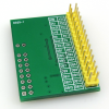
【16位並行模式接線圖】 — AD7606也支持8位匯流排模式,請參見AD7606數據手冊
AD7606模組 MCU側
GND <—– 地
+5V <—– 5V電源
RAGE <—– 可接GPIO也可接固定電平
OS2 <—– 可接GPIO也可接固定電平
OS1 <—– 可接GPIO也可接固定電平
OS0 <—– 可接GPIO也可接固定電平
CVA <—– 接GPIO(輸出)用於啟動AD轉換 【推薦接具有PWM輸出能力的引腳】
CVB <—|
RD <—– 8080匯流排讀信號 NOE
RST <—– GPIO輸出 硬體複位AD606
BUSY —–> GPIO輸入 AD606正在轉換指示。【推薦接具有外部中斷能力的引腳】
CS <—– 8080匯流排片選 NCS
VIO <—– 單片機電源
DB0-DB15 —–> 8080數據匯流排(16位)
FRST 可不接
【SPI介面模式接線圖】
AD7606模組 MCU側
GND <—– 地
+5V <—– 5V電源
RAGE <—– 任意輸出GPIO,可接固定電平
OS2 <—– 任意輸出GPIO,可接固定電平
OS1 <—– 任意輸出GPIO,可接固定電平
OS0 <—– 任意輸出GPIO, 可接固定電平
CVA <—– 接GPIO(輸出)用於啟動AD轉換 【推薦接具有PWM輸出能力的引腳】
CVB <—|
RD/SCLK <—– SPI匯流排時鐘 SCK
RST <—– 任意輸出GPIO, 用於硬體複位AD606
BUSY —–> GPIO輸入, AD606正在轉換指示。【推薦接具有外部中斷能力的引腳】
CS <—– SPI匯流排片選 SCS
VIO <—– 單片機電源
DB7(DOUTA) —–> SPI匯流排數據線MISO
DB14-DB15 可不接
FRST 可不接
【軟體定時採集的實現方案1】 — 我們提供的 spi 的例子採用這種方案 見 bsp_spi_ad7606.c 檔
在定時器中斷服務程式中實現:
定時器中斷ISR:
{
中斷入口;
讀取8個通道的採樣結果保存到RAM; —-> 讀取的是上次的採集結果,對於連續採集來說,是沒有關係的
啟動下次ADC採集;(翻轉CVA和CVB)
中斷返回;
}
定時器的頻率就是ADC採樣頻率。這種模式可以不連接 BUSY 口線。
【軟體定時採集的實現方案2】 — 我們提供的 8080介面例子採用這種方案 見 bsp_ad7606.c 檔
配置CVA CVB 引腳為PWM輸出模式,週期設置為需要的採樣頻率; —> 之後MCU將產生週期非常穩定的AD轉換信號
將BUSY口線設置為中斷下降沿觸發模式;
外部中斷ISR
{
中斷入口;
讀取8個通道的採樣結果保存到RAM;
中斷返回;
}
【軟體定時採集的實現方案1和方案2的差異】
(1)方案1 可以少用 BUSY口線, 但是其他中斷服務程式或者主程序臨時關閉全局中斷時,可能導致ADC轉換週期存在輕微抖動。
(2)方案2 可以確保採集時鐘的穩定性,因為它是MCU硬體產生的。但是需要多接一根 BUSY口線。
原廠驅動資料:https://www.analog.com/cn/products/ad7606.html
1. using high-precision 16-bit ADC chip AD7606
2. 8 analog inputs. 1M ohm impedance. [No negative supply, there is no front-end analog amplifier can be connected directly to the sensor output]
3. the input range of plus or minus 5V, plus or minus 10V. By IO control.
4. Resolution 16.
5. the maximum sampling frequency sampling rate of 200ksps. Supports eight sampling settings file (which can effectively reduce the jitter)
6. built-in benchmark
7. a single 5V power supply
8. SPI Interface, or 16-bit bus interface. Interface IO level can be 5V or 3.3V.
We AD7606 module factory default is 16bit parallel interface.
If SPI interface mode, you need to modify R1 R2 resistor configuration.
(8080 8bit)Parallel Mode Jumper: R1 floating (not stickers), R2 10K resistor paste
SPI interface mode jumper: R1 floating (not stickers), R2 10K resistor paste
AD7606 configuration is very simple, it has no internal registers. Range and over-sampling parameters are controlled via an external IO.
Pulse frequency sampling rate provided by the microcontroller or DSP control.
AD7606 must use a single 5V supply.
Level communication interface between the AD7606 and SCM controlled by VIO pin. That VIO power supply must be connected to the microcontroller can be 3.3V can also be 5V.
Module Pin Description
OS2 OS1 OS2: a combination of state selection oversampling mode.
000 means no oversampling, the maximum sampling rate of 200ksps.
001 represents two times oversampling, which is the hardware inside collected two samples averaging
010 represents four times oversampling, which is the hardware inside collect four samples averaged
011 represents eight times oversampling, which is the hardware inside collected eight samples averaged
100 represents 16 times oversampling, which is the hardware inside collected 16 samples averaged
101 represents 32 times oversampling, which is an internal hardware averaging collected 32 samples
110 represents 64 times oversampling, which is the hardware inside collected 64 samples averaged
Oversampling ratio is higher, the longer the ADC conversion time, the lower the maximum sampling frequency can be obtained.
CVA, CVB: AD conversion start control signal channel 1-4 decision CVA, CVB decided 5-8 channels.
Two signals can stagger a short time, in general, can be CVA, CVB parallel together.
RAGE: Select the range of 0 means plus or minus 5V, 1 indicates negative 10V.
RD: Read signal
RST: Reset signal
Busy: Busy Signal
CS: chip-select signal
FRST: first a channel samples indicating signal
VIO: communication interface level
DB0 – DB15: Data Bus
[16 parallel mode wiring diagram — AD7606 also supports 8-bit bus mode, see the AD7606 data sheet
MCU side AD7606 module
GND <—– ground
+5 V <—– 5V power supply
RAGE <—– can also be connected to the GPIO connected fixed level
OS2 <—– can also be connected to the GPIO connected fixed level
OS1 <—– can also be connected to the GPIO connected fixed level
OS0 <—– can also be connected to the GPIO connected fixed level
CVA <—– access the GPIO (output) is used to start AD conversion [Recommended pick pin with PWM output capability]
CVB <— |
RD <—– 8080 bus read signal NOE
RST <—– GPIO output hardware reset AD606
Busy —–> GPIO input AD606 being converted instructions. [Recommended connection with external pin interrupt capability]
CS <—– 8080 bus chip select NCS
VIO <—– microcontroller power supply
DB0-DB15 —–> 8080 data bus (16)
FRST may take
[SPI interface mode wiring diagram
MCU side AD7606 module
GND <—– ground
+5 V <—– 5V power supply
RAGE <—– any output GPIO, can be accessed by a fixed level
OS2 <—– any output GPIO, can be accessed by a fixed level
OS1 <—– any output GPIO, can be accessed by a fixed level
OS0 <—– any output GPIO, can be accessed by a fixed level
CVA <—– access the GPIO (output) is used to start AD conversion [Recommended pick pin with PWM output capability]
CVB <— |
RD / SCLK <—– SPI bus clock SCK
RST <—– any output GPIO, for hardware reset AD606
Busy —–> GPIO input, AD606 being converted instructions. [Recommended connection with external pin interrupt capability]
CS <—– SPI bus chip select SCS
VIO <—– microcontroller power supply
DB7 (DOUTA) —–> SPI bus data lines MISO
DB14 – DB15 may pick
FRST may take
相關商品
-
MyoWare 2.0 Muscle Sensor Basic Kit 肌電感測器,肌肉信號感測器套件
NT$3,340 未稅MyoWare 2.0 肌肉感測器開發套件是一款與 Arduino 相容的一體化肌電圖 (EMG) 感測器套件,可為您提供 MyoWare 2.0 生態系統的最低限度的功能,以開始測量和可視化肌肉活動。只需扣上 MyoWare 2.0 LED Shield,添加一些 EMG 感測器墊,將感測器連接到肌肉群,然後彎曲即可!
-
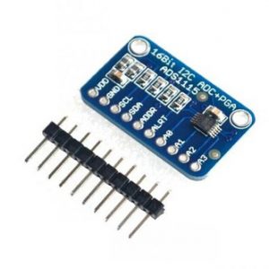
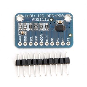
ADS1115 四通道 超小型16位精密模數轉換器(ADC) 開發板模組 16-Bit ADC
- 超小型QFN封裝:ADS1113,ADS1114和ADS1115均為2mm×1,5mm×0.4mm精密模數轉換器(ADC),帶16個
- 寬電源範圍:2.0V至5.5V的分辨率,採用超小型無引線技術
- 低消耗電流:QFN-10封裝或MSOP-10封裝。 ADS1113 / 4/5採用精密,功耗和連續模式設計:僅150μA易於實現。 ADS1113 / 4/5單次模式:自動關機功能,板載參考和振盪器。
- 可編程數據速率:通過I2C兼容串行接口傳輸;可以選擇四個8SPS至860SPS I2C從地址。
- 內部低漂移ADS1113 / 4/5採用單電源供電,電壓範圍為2.0V至5.5V。
- 內部振盪器ADS1113 / 4/5可以按速率執行轉換
NT$295NT$200 未稅 -
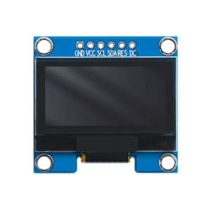
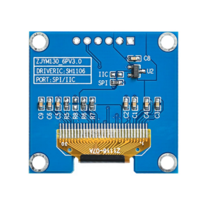
1.3吋OLED 液晶屏顯示模組128×64 黑底藍字 SH1106 SPI 6針
NT$160 未稅- 尺寸:1.3寸
- 材料:PM OLED
- 分辨率:28*64
- 控制晶片:SH1106
- 顯示區域:29.42×14.7(mm)
- PCB尺寸:35.4×33.5(mm)
-
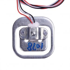
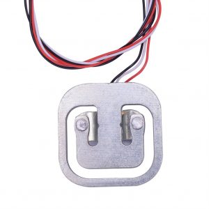
50kg秤重感測器 人體秤50KG電阻應變半橋式感測器 2pcs/組
NT$20 未稅本感測器內部是一組半橋應變片,使用方法可以有以下三種:
- 使用一個傳感器配合外接電阻組成全橋測量,量程為一個傳感器的量程:50kg。對外接電阻要求較高。
- 使用二個傳感器組成全橋測量,量程為兩個傳感器的量程之和:50kgx2=100kg
- 使用四個傳感器組成全橋測量,量程為四個傳感器的量程之和:50kgx4=200kg
-
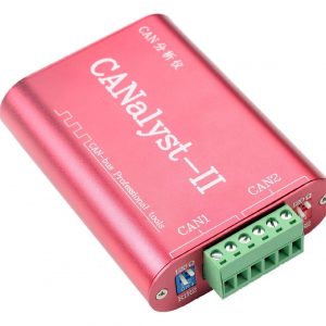
創芯原廠 CANalyst-II USB to CAN Analyzer USB 轉 CAN 分析儀 工業級隔離 USBcan2 轉換器 USB轉CAN 兼容zlg
NT$1,800 – NT$2,060 未稅CANPro 協議分析平台軟件為CANalyst-II的標配軟件,適用於Windows XP, Windows 7/8
支持CAN2.0A/2.0B
能以歷史記錄和新記錄兩種方式顯示CAN幀或協議報文
支持iCAN、DeviceNet、CANopen、SAE J1939等基於CAN-bus網絡的高層協議的分析
用戶可自定義基於CAN-bus網絡的高層協議
可發送協議幀,進行模擬操作 -
Grove – TDS Sensor 水質感測器(總溶解固體) Seeed
NT$500 未稅Grove-TDS 感測器檢測水中的總溶解固體 (TDS) 水平,可用於指示水質。 Grove-TDS Sensor 可應用於水質探測,例如 TDS 儀表、井水、水族箱、水培等。它支持 3.3/5V 輸入電壓和 0 ~ 2.3V 輸出電壓,可輕鬆相容所有 Arduino 板。 該傳感器還提供防水探頭,使測試過程更容易處理。
-
Gravity: MAX30102 心率血氧感測器 (I2C/UART) DFRobot
此Gravity: MAX30102 心率血氧感測器模組搭載了美信(maxim)的 MAX30102 心率血氧晶片和一顆集成心率血氧演算法的微控制器,可以直接輸出心率血氧數值。MAX30102 採用PPG光電容積脈搏波描記法(PhotoPlethysmoGraphy)測量資料,微控制器對這些資料進行處理運算過後得到心率血氧數值,再通過I2C或UART介面輸出,大大降低了感測器的使用難度和對主控的資源佔用。
NT$860NT$800 未稅 -
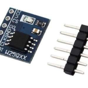
華邦 W25Q128 128Mbit 16MByte FLASH 儲存模組 DataFlash SPI 接口 串列快閃記憶體模組
支援 Arduino FLASH儲存模組,使用靈活,操作方便, 含原廠文件與 Arduino 範例與函數庫。
W25QXX系列是華邦公司推出的大容量SPI FLASH 產品
NT$114NT$80 未稅 -
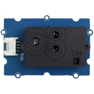
Grove – CO2 & Temperature & Humidity Sensor 二氧化碳+溫度濕度感測器 for Arduino (SCD30)
這一款 3 合 1 Arduino 感測器,可以測量二氧化碳、溫度和濕度。基於 Sensirion SCD30 的非色散紅外 (NDIR) 二氧化碳感測器,具有高精度和寬測量精度,可在 400ppm 至 10’000ppm 之間達到 ±(30 ppm + 3%)。如果您不是在尋找簡單的 Arduino 溫度感測器或 CO2 傳感器,而是為您的 Arduino 氣象站或其他環境項目尋找多功能感測器,這將是一個完美的選擇。
NT$2,381NT$2,140 未稅 -
20×4 SerLCD – RGB Backlight (Qwiic)